
Full resolution (JPEG) - On this page / på denna sida - A Linear Selection Memory with Transistor Driving Circuits, by Bengt Jiewertz
<< prev. page << föreg. sida << >> nästa sida >> next page >>
Below is the raw OCR text
from the above scanned image.
Do you see an error? Proofread the page now!
Här nedan syns maskintolkade texten från faksimilbilden ovan.
Ser du något fel? Korrekturläs sidan nu!
This page has never been proofread. / Denna sida har aldrig korrekturlästs.
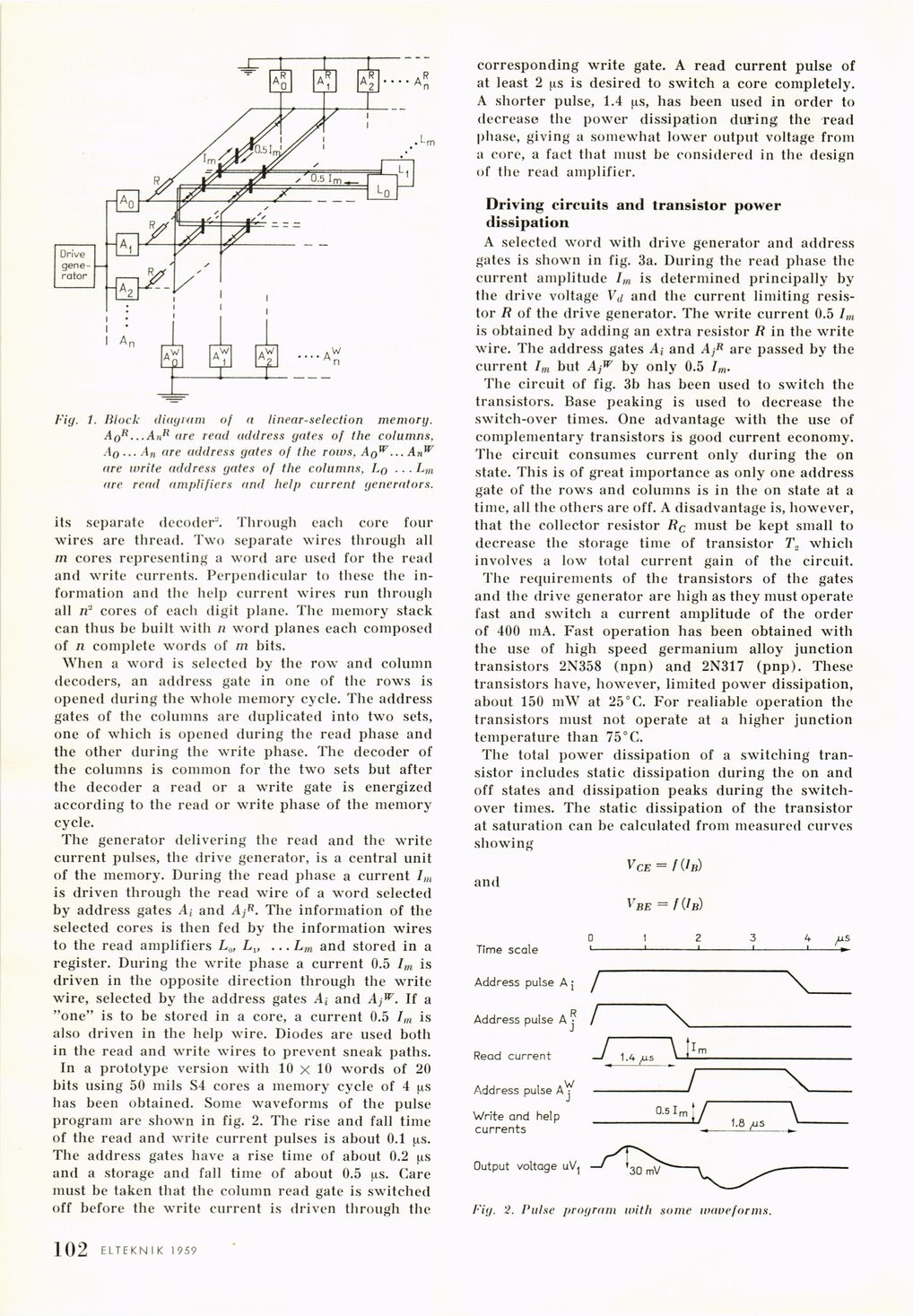
Fig. 1. Block diagram of a linear-selection memory.
Aqr...AnR are read address gates of the columns,
Ao..-An are address gates of the roms, Aqw... Anw
are write address gates of the columns, Lq .. . Lm
are read amplifiers and help current generators.
its separate decoder2. Through each core four
wires are thread. Two separate wires through all
m cores representing a word are used for the read
and write currents. Perpendicular to these the
information and the help current wires run through
all n’J cores of each digit plane. The memory stack
can thus be built with n word planes each composed
of ii complete words of in bits.
When a word is selected by the row and column
decoders, an address gate in one of the rows is
opened during the whole memory cycle. The address
gates of the columns are duplicated into two sets,
one of which is opened during the read phase and
the other during the write phase. The decoder of
the columns is common for the two sets but after
the decoder a read or a write gate is energized
according to the read or write phase of the memory
cycle.
The generator delivering the read and the write
current pulses, the drive generator, is a central unit
of the memory. During the read phase a current Im
is driven through the read wire of a word selected
by address gates At and A;R. The information of the
selected cores is then fed by the information wires
to the read amplifiers L0, Llt ... Lm and stored in a
register. During the write phase a current 0.5 Im is
driven in the opposite direction through the write
wire, selected by the address gates A; and Ajw. If a
"one" is to be stored in a core, a current 0.5 Im is
also driven in the help wire. Diodes are used both
in the read and write wires to prevent sneak paths.
In a prototype version with 10 x 10 words of 20
bits using 50 mils S4 cores a memory cycle of 4 ^s
has been obtained. Some waveforms of the pulse
program are shown in fig. 2. The rise and fall time
of the read and write current pulses is about 0.1 [.is.
The address gates have a rise time of about 0.2 us
and a storage and fall time of about 0.5 jas. (’are
must be taken that the column read gate is switched
off before the write current is driven through the
corresponding write gate. A read current pulse of
at least 2 ^.s is desired to switch a core completely.
A shorter pulse, 1.4 |xs, has been used in order to
decrease the power dissipation during the read
phase, giving a somewhat lower output voltage from
a core, a fact that must be considered in the design
of the read amplifier.
Driving circuits and transistor power
dissipation
A selected word with drive generator and address
gates is shown in fig. 3a. During the read phase the
current amplitude lm is determined principally by
the drive voltage Vj and the current limiting
resistor R of the drive generator. The write current 0.5 Im
is obtained by adding an extra resistor R in the write
wire. The address gates At and AjR are passed by the
current Im but Ajw by only 0.5 Im.
The circuit of fig. 3b has been used to switch the
transistors. Base peaking is used to decrease the
switch-over times. One advantage with the use of
complementary transistors is good current economy.
The circuit consumes current only during the on
state. This is of great importance as only one address
gate of the rows and columns is in the on state at a
time, all the others are off. A disadvantage is, however,
that the collector resistor Rc must be kept small to
decrease the storage time of transistor T2 which
involves a low total current gain of the circuit.
The requirements of the transistors of the gates
and the drive generator are high as they must operate
fast and switch a current amplitude of the order
of 400 mA. Fast operation has been obtained with
the use of high speed germanium alloy junction
transistors 2N358 (npn) and 2N317 (pnp). These
transistors have, however, limited power dissipation,
about 150 mW at 25°C. For realiable operation the
transistors must not operate at a higher junction
temperature than 75 °C.
The total power dissipation of a switching
transistor includes static dissipation during the on and
off states and dissipation peaks during the
switchover times. The static dissipation of the transistor
at saturation can be calculated from measured curves
showing
Vce = fun)
and
vbe = /(/ß)
Fig. 2. Pulse program with some wave forms.
] 102 ELTEKN I K 1959
<< prev. page << föreg. sida << >> nästa sida >> next page >>